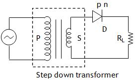
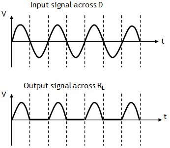
^Full wave rectifier
^Full wave rectifier

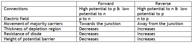
If during the positive half cycle of the input the end A becomes positive and the end B becomes negative with respect to the center tap C then diode D1 gets towards biased and conducts current D2 is reverse biased and does not conduct. During the negative half cycle the diode D1 gets reverse biased and does not conduct & D2 conducts current. As during both half cycles of input ac the current through load RL flows in the same direction F to C.