Posts

^Solar or photovoltaic cells

^Solar or photovoltaic cells

A solar cell is a pn junction diode generally made from Si or GaAs. It works on following three basic processes: generation, separation and collection:

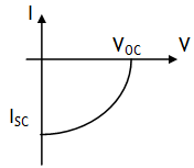
When sun light of energy   E > Eg falls near the junction (area large) they excite the electrons from VB to CB, leaving behind equal number of holes in the VB. These photo generated electron – hole pairs generated in the depletion region move in opposite directions due to the barrier electric field (electrons move towards n side and holes move towards p side of the junction) & are collected near the side of the diode, which makes the p – side a positive electrode & the n – side a negative electrode & thus a photovoltaic potential difference is developed across the junction. If external load is connected across a solar cell a photocurrent IL starts flowing through it. This current is proportional to the intensity of the illumination falling on the diode.

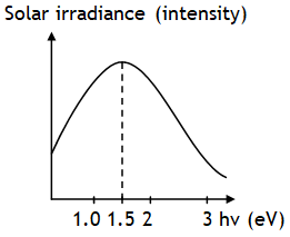
Solar intensity received is maximum near 1.5 eV. As, for photo excitation E > Eg, so, semiconductor with band gap energy Eg ~ 1.5 eV or lower gives better solarconversion energy & thus are ideal materials for solar cell fabrication. Since Si has Eg ~ 1.1 eV while for GaAs it is ~1.43 eV, so they have relatively higher absorption coefficient than other  materials like CdS or CdSe. This is why Si and GaAs are preferred materials for solar cells. Note that sunlight is not always required for a solar cell.

Any light with photon energies greater than the band gap will do.

Solar cells are used to power electronic devices in satellites and space vehicles and also as power supply to some calculators.

^LED

^LED

LED means light emitting diode. It is usually heavily doped. On forward biasing the diode majority carriers combine with minority carriers near the junction & emit energy (spontaneous radiation) in the form of visible light. Increase in the forward current results in decrease of light intensity. LEDs are biased such that the light emitting efficiency is maximum. The V-I characteristics of a LED is similar to that of a Si junction diode. But the threshold voltages are much higher and slightly different for each colour. The reverse breakdown voltages of LEDs are very low, typically around 5V. So care should be taken that high reverse voltages do not appear across them. LEDs must at least have a band gap of 1.8 eV (spectral range of visible light is from about 0.4 mm to 0.7 mm, i.e., from about 3 eV to 1.8 eV). The compound semiconductor Gallium Arsenide – Phosphide (GaAs1-xPx) is used for making LEDs of different colours. GaAs0.6 P0.4 (Eg ~ 1.9 eV) is used for red LED. Si (Eg ~ 1 eV), Ge (Eg ~ 0.9 eV), GaAs (Eg ~ 1.4 eV) are used for making infrared LED. LEDs are used in display of watches, calculators, telephones, measuring instruments etc., remotes of electronic devices, decorative items.

^Ripple factor

^Ripple factor

The output obtained from a rectifier is the superposition of both ac & dc components. The ratio of ac component to the dc component in the rectified output is called the ripple factor it decides the effectiveness of a rectifier. i.e.

ac power input

It is the effective input power i.e.

dc power output

It is the effective output power across the load i.e.

Rectifier efficiency

It is defined as the ratio of dc output power to the applied ac input power i.e.

^Virtual or rms value of current

^Virtual or rms value of current

For a given time interval it is that much direct current which produces the same heat in a resistance as is produced by the varying current in the same resistance for the same time interval, it is

^dc or average value of current

^dc or average value of current

For a given time interval it is that much direct current which sends the same charge through a resistance as is sent by the varying current through the same resistance for the same time interval, it is

^Terms associated with a rectifier Output current in load for one complete cycle

^ Terms associated with a rectifier Output current in load for one complete cycle

Let Input voltage V = Vo sin ωt is applied to a rectifier, then

For a half wave rectifier

Let rf & RL are the forward resistance of the junction and the load resistance respectively

Then peak value of output current will be

For a full wave rectifier

The negative sign indicates that the current due to the second diode flows through the circuit a time T/2 later than the current due to the first diode.


^Bridge rectifier

^Bridge rectifier

It uses four diodes is shown in figure.

For positive half of input cycle diodes D1 and D2 are forward biased and D3 and D4 are reverse biased. So D1 and D2 conduct but D3 and D4 don’t. Current through RL flows from X to Y.

For negative half of input cycle D3 and D4 are forward biased and D1 & D2 are reverse biased. So in this half cycle D3 and D4 conduct but D1 and D2 do not. Current again flows from X to Y through RL.

Thus, we see that current through RL always flows in one direction from X to Y.

^Series inductor filter

^Series inductor filter

The resistance offered by an inductor is XL = 2 πfL, it offers low resistance to low frequency currents (i.e. dc) thus only the low frequency currents pass through it & hence pass through RL. High frequency currents are blocked & don’t appear in the output.

^Parallel capacitor filter

^Parallel capacitor filter 

The resistance offered by a capacitor is 
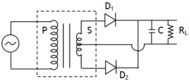
it offers high resistance to low frequency currents (i.e. dc) or it blocks low frequency currents through it. As a result these low frequency currents can pass through RL only.


^Filter circuits

^Filter circuits

The output obtained from a junction diode rectifier is unidirectional but pulsating. This can be considered as the sum of a dc signal superimposed with many ac signals of different harmonic frequencies. We can obtain dc voltage by filtering out the ac components using two types of simple filter circuits.

error: Content is protected !!
Call 9872662552