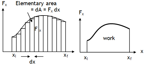
is read as work done by a force ‘Fx’ in moving an object form point A to point B is equal to area under F – x graph bounded with the displacement – axis under position limits of the point A & B.
Conventionally upward areas are +ve & downward –ve.
/wp-content/uploads/2021/04/logo-2.png00kp-web-admin/wp-content/uploads/2021/04/logo-2.pngkp-web-admin2022-01-18 15:11:042022-01-18 15:11:04^Calculating work from F - x graph
If two blocks of highly polished steel were cleaned and placed together in a perfect vacuum, they would weld themselves together and become one block of steel. This is called cold welding. In reality, small amounts of air, moisture, and contaminants accumulate on surfaces and prevent such “ideal” interactions.
/wp-content/uploads/2021/04/logo-2.png00kp-web-admin/wp-content/uploads/2021/04/logo-2.pngkp-web-admin2022-01-17 19:18:042022-01-17 19:18:04^What is cold welding
Three identical cars A, B and C are moving at the same uniform, speed on three bridges. The car A goes on a plane bridge, B on a bridge convex upward and C goes on a bridge concave upward . Let NA, NB and NC be the normal forces exerted by the cars on the bridges when they are at the middle of bridges.
/wp-content/uploads/2021/04/logo-2.png00kp-web-admin/wp-content/uploads/2021/04/logo-2.pngkp-web-admin2022-01-15 18:48:162022-01-15 18:48:16^Cars on curved bridges
Basic building blocks of digital electronics made of semiconducting material & used to control the flow of information from input to output in a logical manner & are used in calculators, digital watches, computers, robots, industrial control systems, and in telecommunications.
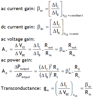
Transconductance is also called mutual conductance.
As β > > α, thus the ac power gain of a CEA is much larger than that of a CBA. Remember the transistor is not generating any power. The energy for the higher ac power at the output is supplied by the battery.
Saturation state:
Both the junction are forward biased & here IC is maximum & does not depend on the input current IB.
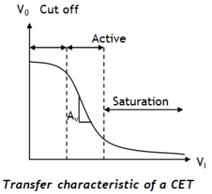
Cut off state: Both the junctions are reverse biased as a result IC = 0. Between cut off & saturation state a transistor works as switch as here it turns over rapidly from OFF state (i.e. IC = 0 or cut off) to the ON state (i.e. IC is maximum or saturation state).
Active state: Emitter base junction is forward biased and the collector base junction is reverse biased. A transistor works as an audio amplifier in this regions.
Relation between α and β:
As the value of IB is about 1 – 5 % of IE or IC is 95 – 99 % of IE, α is about 0.95 and 0.99 and β is about 20 to 100. It is found that α and β are independent of current if the emitter base junction is forward biased and the collector base junction is reverse biased. Also the above definitions of α and β do not hold when both the junctions of a transistor are forward biased or reverse biased.
The CE configuration is frequently used as it gives high current gain as well as voltage gain.
Emitter is the section on one side of transistor that supplies charge carriers. It is of moderate size & heavily doped. Collector is the section on the other side of transistor that collects the charge carriers. It is moderately doped but larger in size. Base is the middle section of transistor that forms two pn junctions with emitter and collector. It is very thin and lightly doped so as to pass most of the emitter injected charge carriers to the collector.
A transistor is also called Bipolar Junction Transistor (BJT), as in it current is due to both majority & minority charge carriers.
Input of a transistor is always forward biased, output is reverse biased & the common terminal is grounded.
Current in both npn & pnp transistor is IE = IB + IC. As the base current IB is very small thus IE » IC.. A transistor transfer almost the same electric current from low resistance path to high resistance path and hence is named as transistor. This transistor action makes it useful in transistor amplifier.
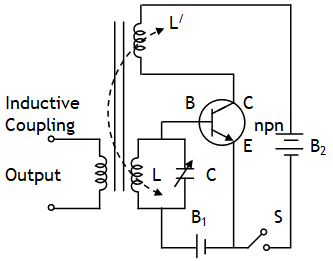
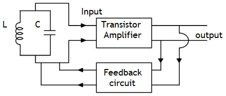
A transistor can be used as a switch, amplifier, oscillator & NOT gate.
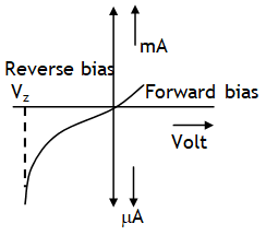
It is a specially designed junction diode, which can operate in the reverse breakdown voltage region continuously without being damaged. In forward bias behaves like ordinary diode. Zener diode does not gets damaged at breakdown voltage, but it does so at some higher reverse voltage, known as its ‘burn out value’. The magnitude of zener voltage VZ can be decreased by increasing doping level in p and n type materials of zener diode.
I – V characteristics of a Zener diode are as shown. For a voltage more than zener breakdown voltage current through diode increases without increase in voltage across it. This feature is exploited to provide voltage stabilization across a circuit.
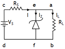
Suppose a load RL connected between a & b is connected to a fluctuating dc voltage supply Vs between c & d. Let the load can’t tolerate a voltage VL but the supply Vs can be more than VL. To protect the load from any increase voltage a zener diode of breaking voltage VZ = VL is connected to the input supply with a safety resistor RS in the input loop.
If at any time VZ increases than VL the zener diode works in the breakdown region increasing the current through it without increasing the voltage across it & thus the load always remains protected.
Our objective is to create a situation where students will find Physics interesting & the strongest subject helping them to achieve top ranks in competitive exams.