Posts

^Zener diode

^Zener diode

It is a specially designed junction diode, which can operate in the reverse breakdown voltage region continuously without being damaged.  In forward bias behaves like ordinary diode.  Zener diode does not gets damaged at breakdown voltage, but it does so at some higher reverse voltage, known as its ‘burn out value’. The magnitude of zener voltage VZ can be decreased by increasing doping level in p and n type materials of zener diode.

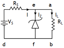
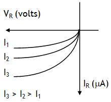
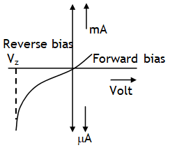
I – V characteristics of a Zener diode are as shown. For a voltage more than zener breakdown voltage current through diode increases without increase in voltage across it. This feature is exploited to provide voltage stabilization across a circuit.

Suppose a load RL connected between a & b is connected to a fluctuating dc voltage supply Vs between c & d. Let the load can’t tolerate a voltage VL but the supply Vs can be more than VL. To protect the load from any increase voltage a zener diode of breaking voltage VZ = VL is connected to the input supply with a safety resistor RS in the input loop.

If at any time VZ increases than VL the zener diode works in the breakdown region increasing the current through it without increasing the voltage across it & thus the load always remains protected.

^Photodiodes

^Photodiodes

Light incident near the junction of reverse biased (because the fractional change due to the photo-effects on the minority carrier dominated reverse bias current is more easily measurable than the fractional change in the forward bias current) diode produce electron hole pairs which are moved by the junction electric field (electrons towards n end & holes near the p end).

Thus p-side becomes positive and n-side becomes negative giving rise to emf. When an external load is connected, a current flows which can be controlled by changing the intensity of light falling on it. It is used in, light operated switches, optical counters, reproduction of sound from film in move projectors & in photo detectors to detect radiations.

^Solar or photovoltaic cells

^Solar or photovoltaic cells

A solar cell is a pn junction diode generally made from Si or GaAs. It works on following three basic processes: generation, separation and collection:

When sun light of energy   E > Eg falls near the junction (area large) they excite the electrons from VB to CB, leaving behind equal number of holes in the VB. These photo generated electron – hole pairs generated in the depletion region move in opposite directions due to the barrier electric field (electrons move towards n side and holes move towards p side of the junction) & are collected near the side of the diode, which makes the p – side a positive electrode & the n – side a negative electrode & thus a photovoltaic potential difference is developed across the junction. If external load is connected across a solar cell a photocurrent IL starts flowing through it. This current is proportional to the intensity of the illumination falling on the diode.

Solar intensity received is maximum near 1.5 eV. As, for photo excitation E > Eg, so, semiconductor with band gap energy Eg ~ 1.5 eV or lower gives better solarconversion energy & thus are ideal materials for solar cell fabrication. Since Si has Eg ~ 1.1 eV while for GaAs it is ~1.43 eV, so they have relatively higher absorption coefficient than other  materials like CdS or CdSe. This is why Si and GaAs are preferred materials for solar cells. Note that sunlight is not always required for a solar cell.

Any light with photon energies greater than the band gap will do.

Solar cells are used to power electronic devices in satellites and space vehicles and also as power supply to some calculators.

^LED

^LED

LED means light emitting diode. It is usually heavily doped. On forward biasing the diode majority carriers combine with minority carriers near the junction & emit energy (spontaneous radiation) in the form of visible light. Increase in the forward current results in decrease of light intensity. LEDs are biased such that the light emitting efficiency is maximum. The V-I characteristics of a LED is similar to that of a Si junction diode. But the threshold voltages are much higher and slightly different for each colour. The reverse breakdown voltages of LEDs are very low, typically around 5V. So care should be taken that high reverse voltages do not appear across them. LEDs must at least have a band gap of 1.8 eV (spectral range of visible light is from about 0.4 mm to 0.7 mm, i.e., from about 3 eV to 1.8 eV). The compound semiconductor Gallium Arsenide – Phosphide (GaAs1-xPx) is used for making LEDs of different colours. GaAs0.6 P0.4 (Eg ~ 1.9 eV) is used for red LED. Si (Eg ~ 1 eV), Ge (Eg ~ 0.9 eV), GaAs (Eg ~ 1.4 eV) are used for making infrared LED. LEDs are used in display of watches, calculators, telephones, measuring instruments etc., remotes of electronic devices, decorative items.

^Ripple factor

^Ripple factor

The output obtained from a rectifier is the superposition of both ac & dc components. The ratio of ac component to the dc component in the rectified output is called the ripple factor it decides the effectiveness of a rectifier. i.e.

ac power input

It is the effective input power i.e.

dc power output

It is the effective output power across the load i.e.

Rectifier efficiency

It is defined as the ratio of dc output power to the applied ac input power i.e.

^Intrinsic SCs

^Intrinsic SCs

At 0 K the VB of an intrinsic semiconductor is completely filled with the electrons while the conduction band is completely empty as a result a SC behaves like an insulator at 0 K temperature.

However at higher temperatures say at room temperature some of the electrons from the VB gain sufficient thermal energy & jump to CB & occupy some level in the CB in accordance with the extent of the excitation energy. This is called thermal agitation. The vacant spaces left behind in the VB are called holes.

The vacancy of an electron with an effective positive electronic charge is called a hole. It behaves as an apparent free particle with a charge +e. For a intrinsic SC ne = nh = ni

On applying external electric field electrons in the CB start drifting in a direction opposite to the electric field & holes in the VB start drifting in the direction of the electric field due to the force  exerted by the electric field as shown in the diagram.

^Energy bands in solids

^Energy bands in solids

Energy levels of electrons in an isolated atom are well defined & discrete, however the valence energy levels get modified drastically when atoms interact to form the lattice. If N atoms interact, then total 8 N energy valence energy levels are available which split in two bands (called VB & CB) separated by energy gap (called Eg) as shown in the diagram.

As E(Ge) < E(Si), thus Ge is preferred in making semi conducting devices.

^Semiconductors

^Semiconductors

Semiconductors (e.g. Si, Ge) belong to 14th group, thus have 4 valence electrons & hence from covalent bonds (temperature sensitive).  

^Absorption radiations

^Absorption radiations

Radiations are absorbed by the materials according to the relation:  I =  I0 e X  

Here    μ  = absorption coefficient

I = intensity after penetrating the material through ‘x’ thickness of material

I0 = intensity of the radiation before penetrating

Absorption coefficient is highest for Pb.

^Commonly used abbreviations

^Commonly used abbreviations

1. R: Roentgen

2. Rad:  Radiation absorbed dose

3. rem: Roentgen equivalent in man

4. RBE: Relative biological effectiveness

error: Content is protected !!
Call 9872662552