Basic building blocks of digital electronics made of semiconducting material & used to control the flow of information from input to output in a logical manner & are used in calculators, digital watches, computers, robots, industrial control systems, and in telecommunications.
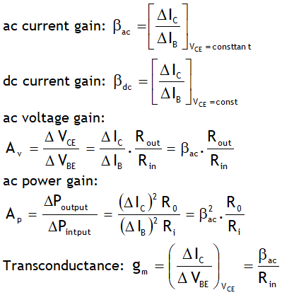
Transconductance is also called mutual conductance.
As β > > α, thus the ac power gain of a CEA is much larger than that of a CBA. Remember the transistor is not generating any power. The energy for the higher ac power at the output is supplied by the battery.
Saturation state:
Both the junction are forward biased & here IC is maximum & does not depend on the input current IB.
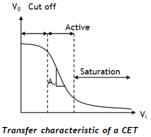
Cut off state: Both the junctions are reverse biased as a result IC = 0. Between cut off & saturation state a transistor works as switch as here it turns over rapidly from OFF state (i.e. IC = 0 or cut off) to the ON state (i.e. IC is maximum or saturation state).
Active state: Emitter base junction is forward biased and the collector base junction is reverse biased. A transistor works as an audio amplifier in this regions.
Relation between α and β:
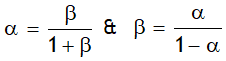
As the value of IB is about 1 – 5 % of IE or IC is 95 – 99 % of IE, α is about 0.95 and 0.99 and β is about 20 to 100. It is found that α and β are independent of current if the emitter base junction is forward biased and the collector base junction is reverse biased. Also the above definitions of α and β do not hold when both the junctions of a transistor are forward biased or reverse biased.
The CE configuration is frequently used as it gives high current gain as well as voltage gain.
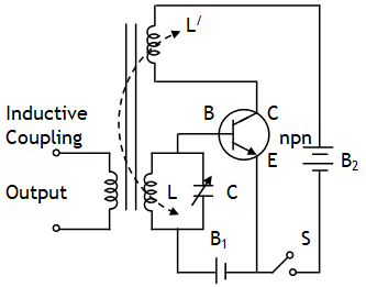
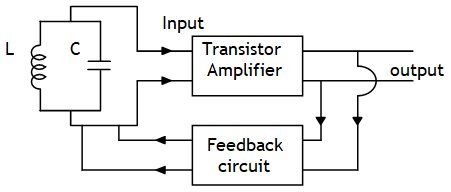
Emitter is the section on one side of transistor that supplies charge carriers. It is of moderate size & heavily doped. Collector is the section on the other side of transistor that collects the charge carriers. It is moderately doped but larger in size. Base is the middle section of transistor that forms two pn junctions with emitter and collector. It is very thin and lightly doped so as to pass most of the emitter injected charge carriers to the collector.
A transistor is also called Bipolar Junction Transistor (BJT), as in it current is due to both majority & minority charge carriers.
Input of a transistor is always forward biased, output is reverse biased & the common terminal is grounded.
Current in both npn & pnp transistor is IE = IB + IC. As the base current IB is very small thus IE » IC.. A transistor transfer almost the same electric current from low resistance path to high resistance path and hence is named as transistor. This transistor action makes it useful in transistor amplifier.
A transistor can be used as a switch, amplifier, oscillator & NOT gate.
It is a specially designed junction diode, which can operate in the reverse breakdown voltage region continuously without being damaged. In forward bias behaves like ordinary diode. Zener diode does not gets damaged at breakdown voltage, but it does so at some higher reverse voltage, known as its ‘burn out value’. The magnitude of zener voltage VZ can be decreased by increasing doping level in p and n type materials of zener diode.
I – V characteristics of a Zener diode are as shown. For a voltage more than zener breakdown voltage current through diode increases without increase in voltage across it. This feature is exploited to provide voltage stabilization across a circuit.
Suppose a load RL connected between a & b is connected to a fluctuating dc voltage supply Vs between c & d. Let the load can’t tolerate a voltage VL but the supply Vs can be more than VL. To protect the load from any increase voltage a zener diode of breaking voltage VZ = VL is connected to the input supply with a safety resistor RS in the input loop.
If at any time VZ increases than VL the zener diode works in the breakdown region increasing the current through it without increasing the voltage across it & thus the load always remains protected.
Light incident near the junction of reverse biased (because the fractional change due to the photo-effects on the minority carrier dominated reverse bias current is more easily measurable than the fractional change in the forward bias current) diode produce electron hole pairs which are moved by the junction electric field (electrons towards n end & holes near the p end).
Thus p-side becomes positive and n-side becomes negative giving rise to emf. When an external load is connected, a current flows which can be controlled by changing the intensity of light falling on it. It is used in, light operated switches, optical counters, reproduction of sound from film in move projectors & in photo detectors to detect radiations.
A solar cell is a pn junction diode generally made from Si or GaAs. It works on following three basic processes: generation, separation and collection:
When sun light of energy E > Eg falls near the junction (area large) they excite the electrons from VB to CB, leaving behind equal number of holes in the VB. These photo generated electron – hole pairs generated in the depletion region move in opposite directions due to the barrier electric field (electrons move towards n side and holes move towards p side of the junction) & are collected near the side of the diode, which makes the p – side a positive electrode & the n – side a negative electrode & thus a photovoltaic potential difference is developed across the junction. If external load is connected across a solar cell a photocurrent IL starts flowing through it. This current is proportional to the intensity of the illumination falling on the diode.
Solar intensity received is maximum near 1.5 eV. As, for photo excitation E > Eg, so, semiconductor with band gap energy Eg ~ 1.5 eV or lower gives better solarconversion energy & thus are ideal materials for solar cell fabrication. Since Si has Eg ~ 1.1 eV while for GaAs it is ~1.43 eV, so they have relatively higher absorption coefficient than other materials like CdS or CdSe. This is why Si and GaAs are preferred materials for solar cells. Note that sunlight is not always required for a solar cell.
Any light with photon energies greater than the band gap will do.
Solar cells are used to power electronic devices in satellites and space vehicles and also as power supply to some calculators.
/wp-content/uploads/2021/04/logo-2.png00kp-web-admin/wp-content/uploads/2021/04/logo-2.pngkp-web-admin2022-01-15 17:34:302022-01-15 17:34:30^Solar or photovoltaic cells
LED means light emitting diode. It is usually heavily doped. On forward biasing the diode majority carriers combine with minority carriers near the junction & emit energy (spontaneous radiation) in the form of visible light. Increase in the forward current results in decrease of light intensity. LEDs are biased such that the light emitting efficiency is maximum. The V-I characteristics of a LED is similar to that of a Si junction diode. But the threshold voltages are much higher and slightly different for each colour. The reverse breakdown voltages of LEDs are very low, typically around 5V. So care should be taken that high reverse voltages do not appear across them. LEDs must at least have a band gap of 1.8 eV (spectral range of visible light is from about 0.4 mm to 0.7 mm, i.e., from about 3 eV to 1.8 eV). The compound semiconductor Gallium Arsenide – Phosphide (GaAs1-xPx) is used for making LEDs of different colours. GaAs0.6 P0.4 (Eg ~ 1.9 eV) is used for red LED. Si (Eg ~ 1 eV), Ge (Eg ~ 0.9 eV), GaAs (Eg ~ 1.4 eV) are used for making infrared LED. LEDs are used in display of watches, calculators, telephones, measuring instruments etc., remotes of electronic devices, decorative items.
Our objective is to create a situation where students will find Physics interesting & the strongest subject helping them to achieve top ranks in competitive exams.